Backend Process Solution
E&R Company is a leading provider of back end process solutions, specializing in advanced laser and plasma technology. Our innovative solutions are designed to enhance productivity and efficiency in various industries. With a commitment to excellence and cutting-edge technology, we deliver superior performance and reliability to meet the evolving needs of our clients.
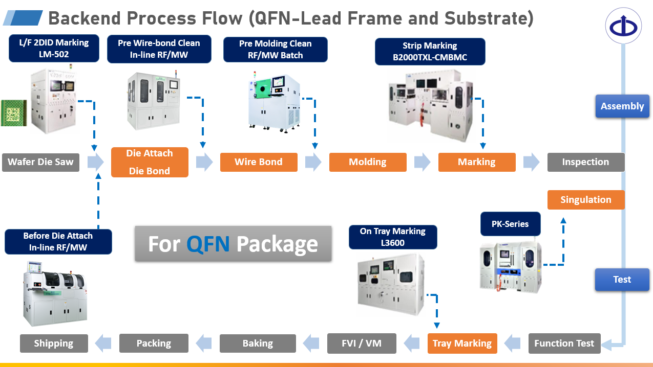
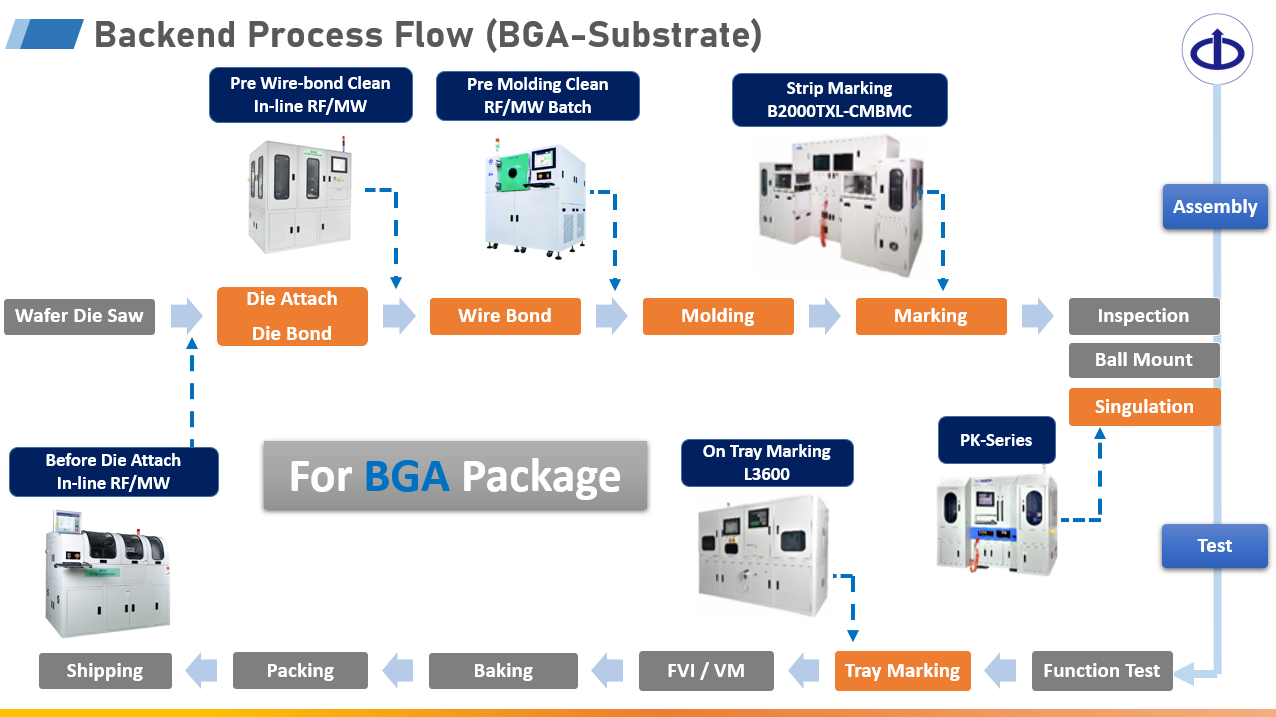
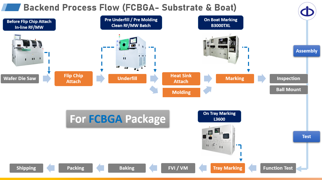
The semiconductor back end process flow typically includes several key stages:
1.Wafer Sawing:
The silicon wafers, on which multiple semiconductor devices are fabricated, are cut into individual chips or die.
2.Die Attach:
Each die is picked and attached to a substrate or lead frame using a bonding material (e.g., adhesive or solder).
3.Wire Bonding:
Thin wires are connected from the die to the substrate or lead frame to establish electrical connections.
4.Molding:
The assembly is encapsulated in plastic or ceramic to protect the die and wire bonds from mechanical damage and environmental factors.
5.Testing (Electrical and Functional):
The ICs undergo rigorous testing to verify their electrical performance and functionality. This includes tests for speed, power consumption, and functionality under various operating conditions.
6.Marking and Singulation:
Each IC is marked with identification codes or logos for traceability and then separated (singulated) into individual units.
7.Final Inspection and Quality Control:
A final inspection is conducted to ensure that all ICs meet the specified quality standards and performance criteria.
8.Packaging:
The ICs are packaged into trays, tubes, or reels for shipment to customers or assembly into electronic products.
9.Shipping:
The packaged ICs are shipped to manufacturers who integrate them into electronic devices such as smartphones, computers, or automotive systems.