Advanced Packaging (AP)
E&R Solution for Advanced Packaging
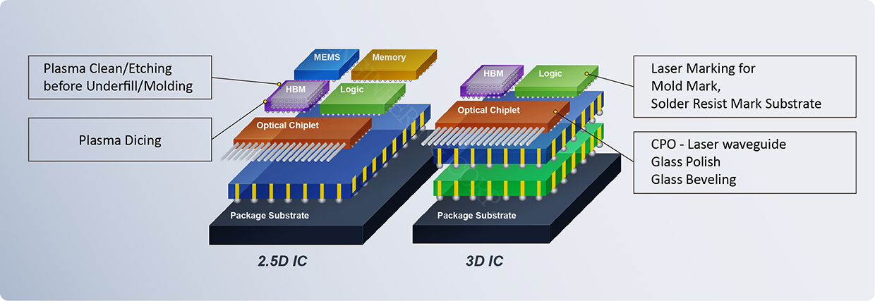
E&R AP (Advanced Packaging) solution focuses on advanced laser and plasma solutions, which can work on the flip-chip platform, including FCBGA, FCCSP, Fan-Out, and Fan-In (Wafer Level).
Machines are manufactured, assembled, and tested in Taiwan, with key components sourced from leading European and USA brands.
Overall, E&R AP solutions have been supplied over 500 sets of tools to major OSATs worldwide, we can help you develop and provide the latest & best solution base on our various experience in semiconductor industry.
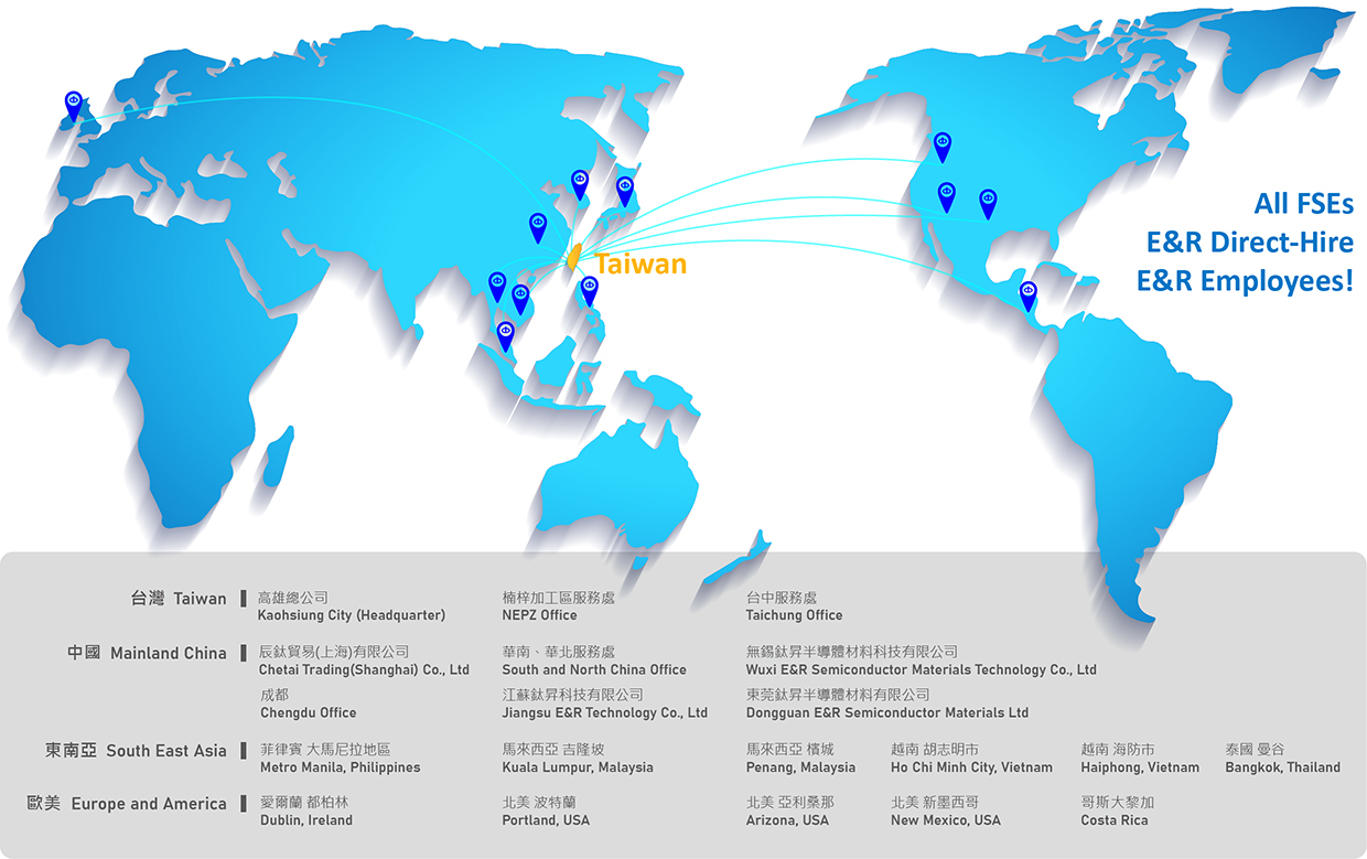
E&R's global service network can also support customers with fast responding time and professional expertises.
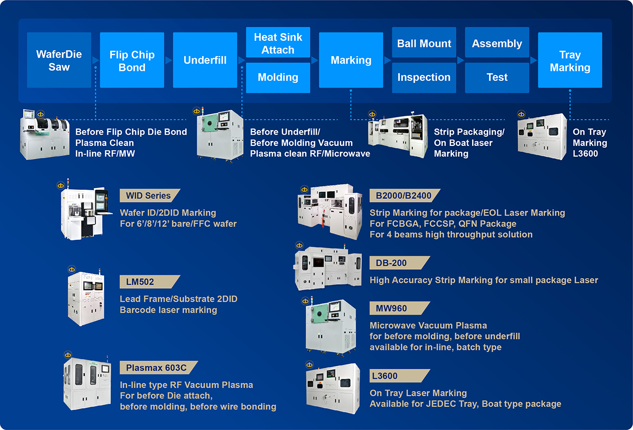
- Laser solution:
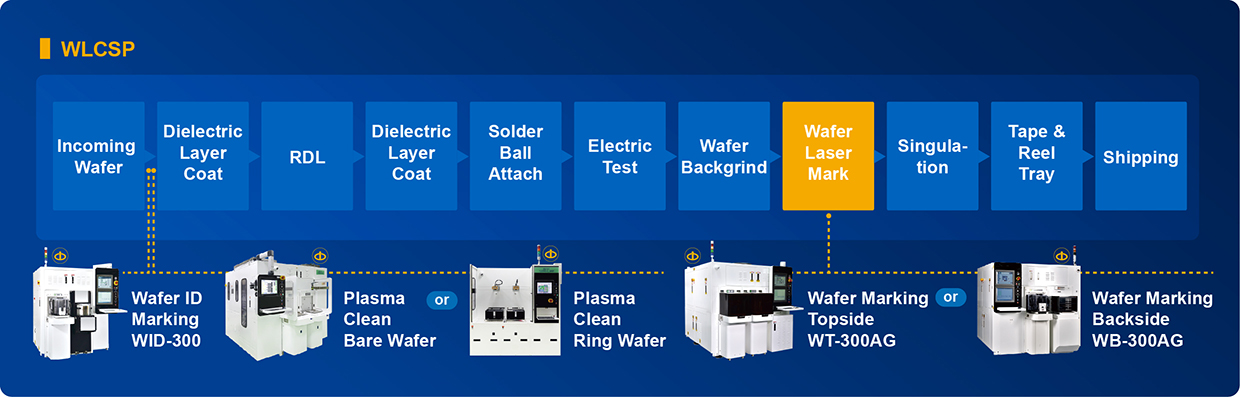
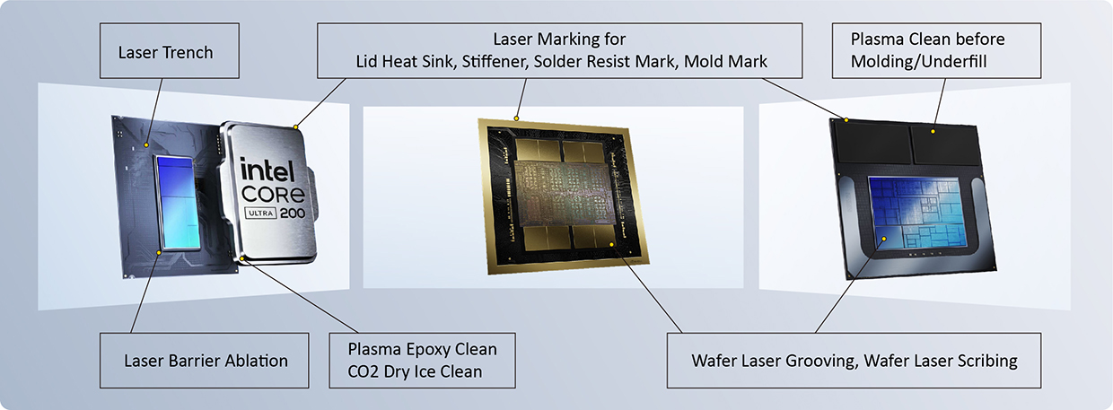
Laser marking for molding compound, substrate solder resist, Lead Frame, Heat sink, stiffener,Wafer ID marking, Wafer backside marking, laser scribing, laser grooving.
- Refer model: LM502, B2000, B2400, WB-200/WB-300, WID Series
- Vacuum Plasma solution:
RF or microwave plasma for before molding/underfill, before wire bonding, surface contamination removal, oxide removal and recast removal.
- Refer model: MW300, MW960, 603/604 service, MW700.
E&R Flip Chip Solution
E&R Backend Process Solution
E&R Technology for AI Product
E&R Technology for 2.5D/3D/CPO
E&R Worldwide Service Centers